


GaN Atomic Layer Etching
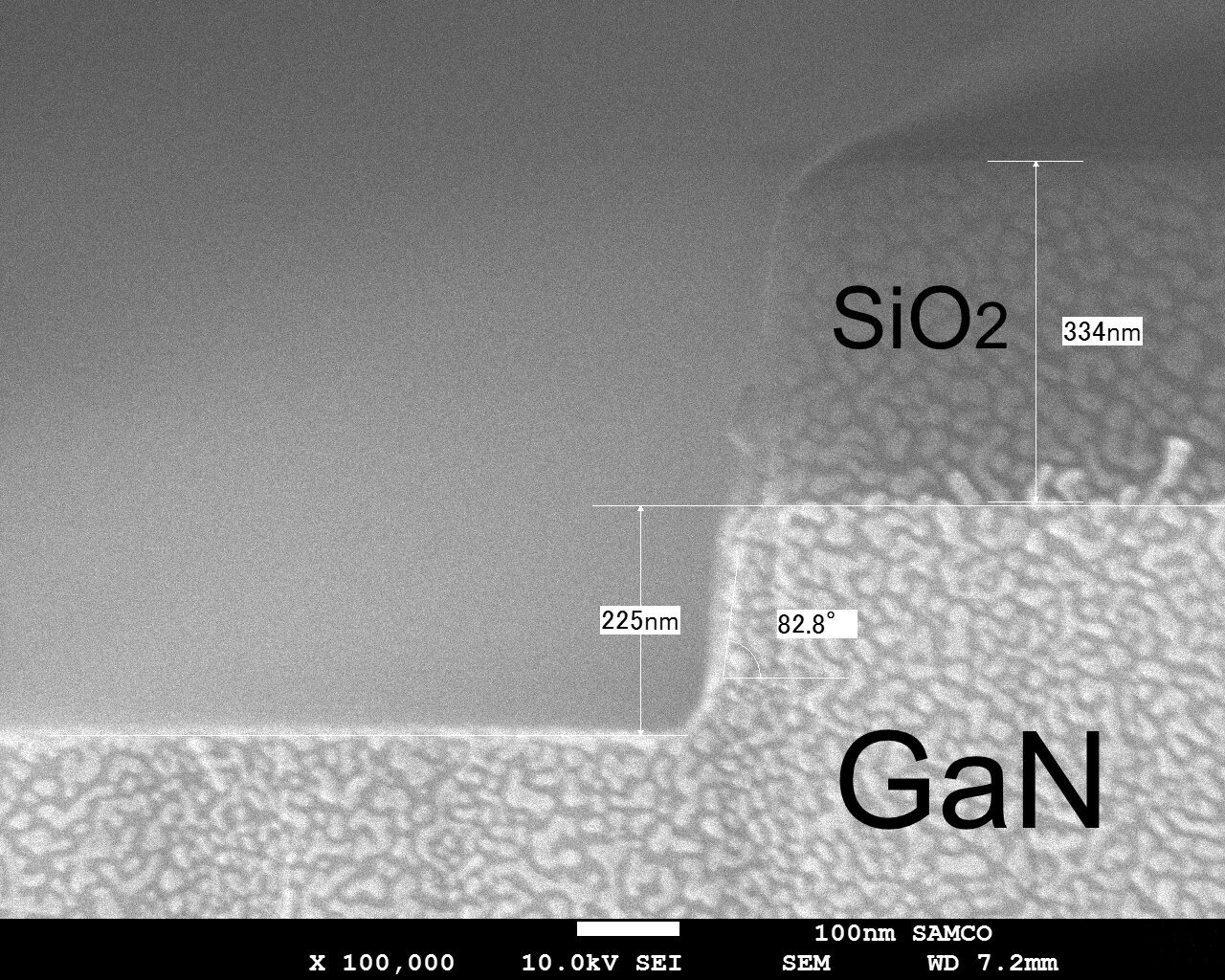
GaN was etched using the Atomic Layer Etching (ALE) method with a SiO2 mask. The trench width is 0.7 µm, yet narrower width process is also possible. The etching rate was about 7.0 Å/cycle, and the etching depth of GaN reached 225 nm. The etching rate could be made as slow as possible with excellent process controllability. Etch selectivity of GaN over SiO2 is 3.5.
This process can be applied to microfabrication of nanopatterns such as photonic crystals, recess etching for GaN HEMTs, and so on.
Tweet