


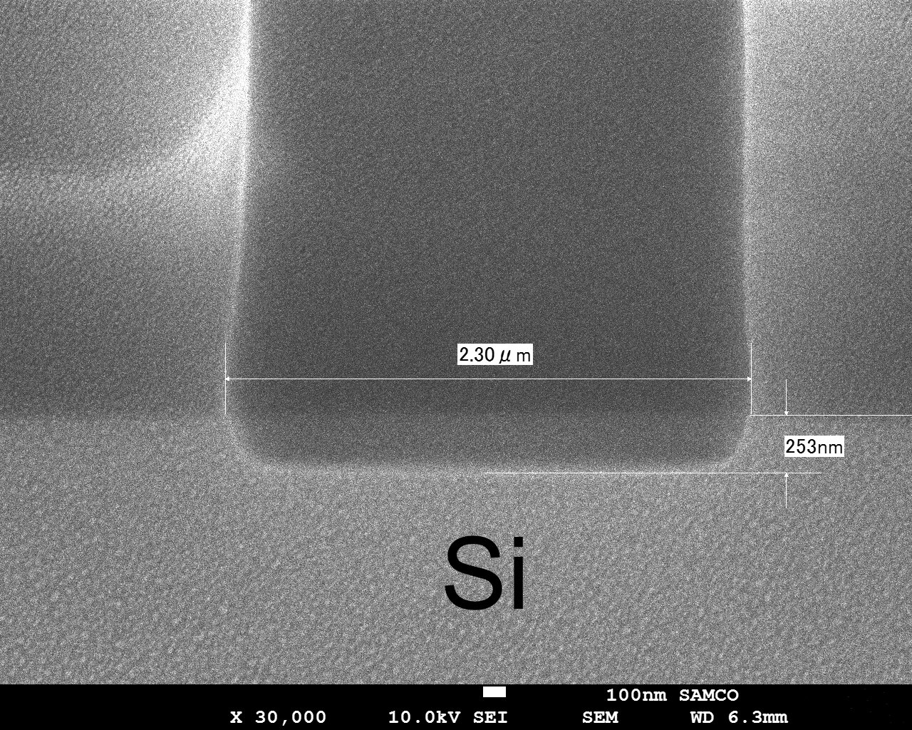
Simultaneous etching of different hole patterns
Si was etched using the Atomic Layer Etching (ALE) method with a photo resist mask. The etching rate was about 12.5 Å/cycle, and the etching depth of Si reached 253 nm. ALE allows for the removal of Si in extremely thin layers, down to the Angstrom level.
In this process, hole diameters of 2um, 20um and 50um were etched simultaneously; the SEM photograph shows the results for hole diameter 2um. The etching rate and depth for all hole diameters were the same. In other words, the use of Atomic Layer Etching suppresses the micro-loading effect.
Tweet