Samco
CCP-RIE Systems
Samco’s Capacitively Coupled Plasma Reactive Ion Etching (CCP-RIE) systems provide stable dry etching solutions for dielectric thin films, fluorinated polymers, and surface modification processes. Utilizing parallel-plate electrode configurations, our CCP platforms generate uniform, low-density plasma across large substrate areas. Designed to meet versatile R&D and production requirements, Samco CCP-RIE systems offer broad operational windows for academic laboratories and semiconductor manufacturing facilities alike.
-
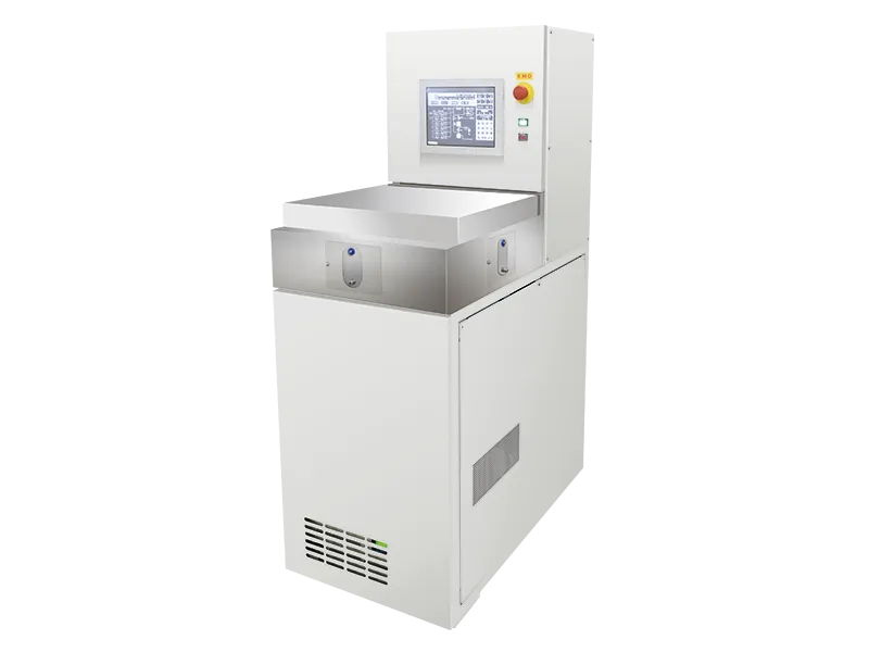
CCP-RIE System RIE-10NR
De Facto Industry Standard
-
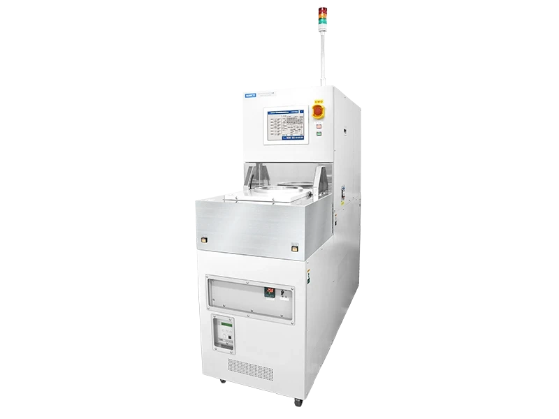
CCP-RIE System RIE-200NL
Load Lock CCP-RIE System
-
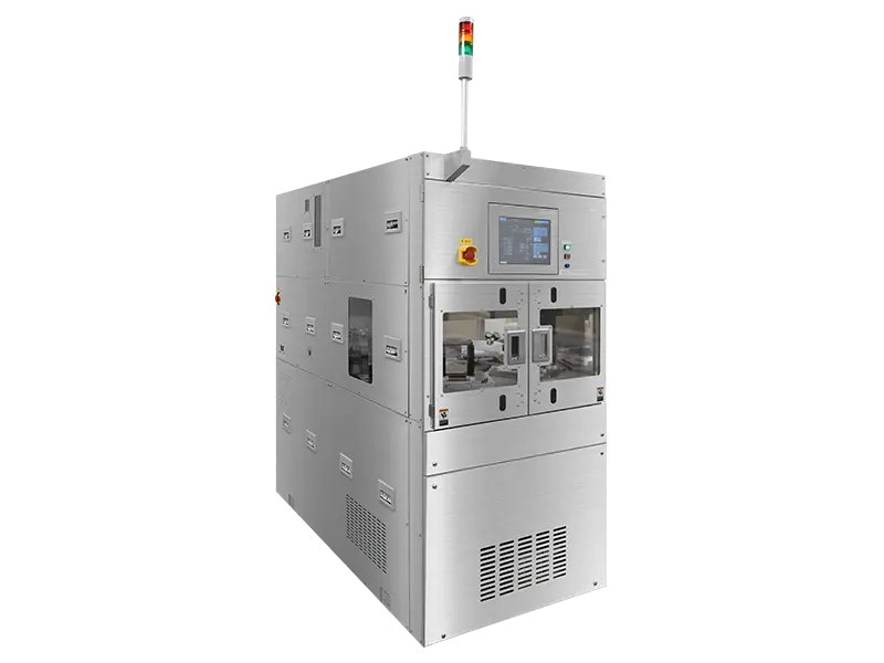
CCP-RIE System RIE-200C
2 Cassettes CCP-RIE System
-
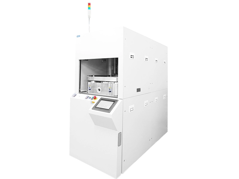
CCP-RIE System RIE-300NR
ø300 mm CCP-RIE System








Features of CCP-RIE Systems
Samco CCP-RIE systems offer broad process latitude for pattern transfer and surface treatment across silicon dioxide (SiO2), silicon nitride (SiN, SiON), fluorinated polymers, and functional glass substrates. Built around a uniform parallel-plate electrode geometry, the system maintains a direct relationship between RF power input and chamber operating pressure to establish a predictable self-bias potential (Vdc). This predictable electric field allows process engineers to tune the balance between chemical reaction rates and physical ion sputtering for shallow recessing, inter-metal dielectric etching, and polymer removal. Supported by fluorine- and chlorine-based gas delivery networks, the system handles open load R&D substrate processing as well as load lock configurations tailored to commercial production requirements.
CCP-RIE Systems FAQ
- What are the main processing characteristics of Capacitively Coupled Plasma (CCP) compared to ICP systems?
- CCP-RIE systems generate low-density plasma across a parallel-plate electrode geometry where plasma density and ion bombardment energy are intrinsically coupled. While ICP systems separate plasma density from substrate bias to maximize etch rates, CCP platforms offer a simple, robust environment well-suited for standard dielectric pattern transfer, polymer removal, and routine dry etching steps.
- How does a CCP-RIE system control the etching mechanism?
- In a CCP configuration, adjusting RF power input and chamber operating pressure directly alters the self-bias voltage (Vdc) at the substrate electrode. Higher RF power increases ion bombardment energy (physical sputtering), while higher pressure increases reactive chemical species concentration. Process engineers tune these two knobs to balance chemical reaction rates with physical directionality.
- What materials are typically processed using Samco CCP-RIE systems?
- Samco CCP-RIE systems process a wide range of dielectric thin films, including silicon dioxide (SiO2), silicon nitride (SiN, SiON), fluorinated polymers, and functional glass substrates. Configured with fluorine- or chlorine-based gas manifolds, the tools deliver predictable etch rates and consistent pattern transfer across inter-metal dielectrics and passivation layers.
- What substrate sizes and package formats are supported by Samco FA-dedicated CCP-RIE platforms?
- To accommodate diverse failure analysis specimens, Samco offers flexible open load tool architectures. The product lineup spans compact systems for standard substrates up to 8-inch (200 mm), dedicated 300 mm platforms, and large-format configurations designed for direct loading of mounted IC packages, oversized FA trays, and irregular specimens.
- Can Samco CCP-RIE platforms process Indium Phosphide (InP) optical gratings using methane-based (CH4/H2) chemistries on load lock tool configurations?
- Yes. Samco load lock CCP-RIE systems accommodate methane-hydrogen (CH4/H2) gas chemistries specifically engineered for precision grating fabrication and shallow ridge etching on Indium Phosphide (InP) optical substrates. By isolating the reaction chamber under continuous vacuum, the load lock configuration prevents atmospheric oxygen and moisture ingress, suppressing background chamber contamination and polymer over-passivation during volatile hydrocarbon plasma exposure. This controlled processing environment enables smooth sidewall morphology, precise depth control, and highly repeatable pitch definition for distributed feedback (DFB) lasers and photonic integrated circuits (PICs).

