


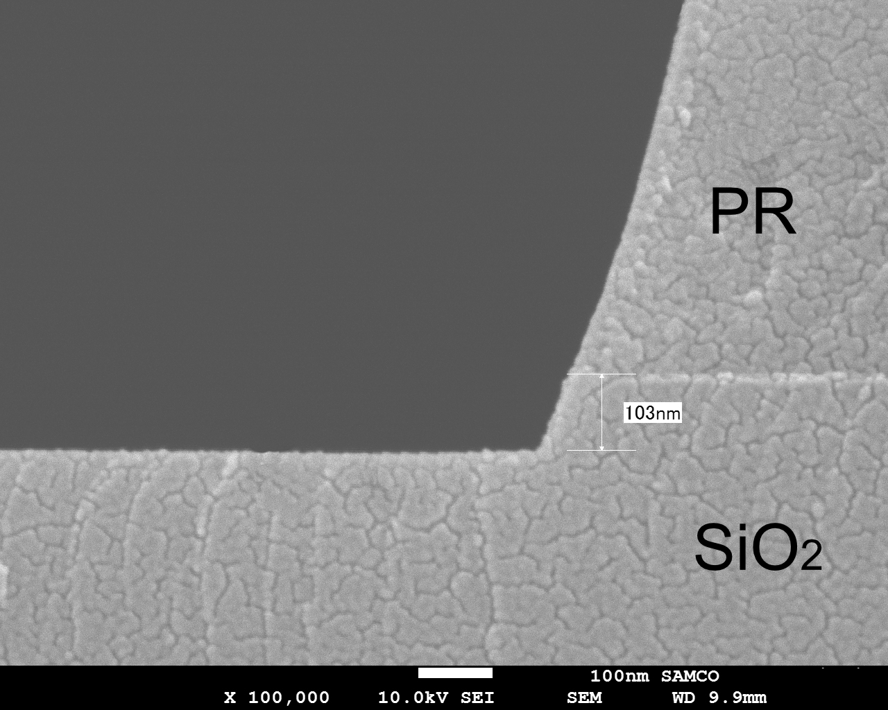
SiO2 was etched using the Atomic Layer Etching (ALE) method with a photo resist mask. The etching rate was about 8.5 Å/cycle, and the etching depth of SiO2 reached 103 nm. ALE allows for the removal of SiO2 in extremely thin layers, down to the Angstrom level. This process could be applied to SiO2/SiN high selectivity etching for Self-Aligned Contact.
Tweet