


1 What is the Bosch Process?
Deep reactive ion etching (DRIE) of silicon to create high aspect ratio microstructures is one of the key processes in the advanced MEMS field and through silicon via (TSV) applications. However, conventional plasma etching processes are designed for etch depths of only a few microns and are lacking in etch-rate and etch mask selectivity. The Bosch process is capable of producing deep features with exceptional anisotropy, etch-rate, and etch mask selectivity.
This process consists of a three-step cycle: Film deposition, bottom film etching, and silicon etching. In the deposition process, a passivation film is deposited on the sidewalls and bottom surface of the trench. In the bottom film etching step, the passivation film on the trench bottom is selectively etched. In the silicon etching step, only the silicon at the trench bottom, where the passivation film has been removed, is etched (Fig. 1).
2 What is the chemical reaction of the Bosch process?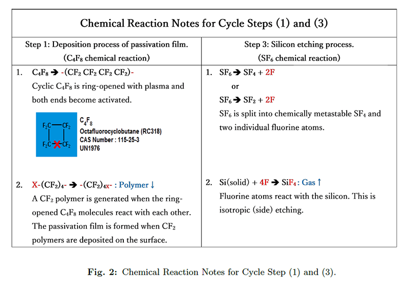
The deposition step typically uses C4F8 gas as the deposition gas. C4F8 is a cyclic molecule (ring shaped), and in plasma, its ring is broken and it becomes a short chain molecule. Both ends of the C4F8 chain are active. The active parts of the chain combine with other molecules and the chain grows in length, attaching to the silicon and forming a membrane. This mem- brane functions as a passivation film during the silicon etching step preventing etching of the sidewalls.
SF6 is usually used as an etching gas for film etching and silicon etching. SF6 dissociates in plasma to form SF4 or SF2 and atomic fluorine that reacts with silicon. Both SF4 and the etching reaction product, SiF4, exist as gases that are evacuated from the chamber. SF4 is so stable that fluorine atoms cannot recombine with it. Therefore, a large amount of atomic fluorine can be produced and participates in the etching reaction.
CF4 decomposes to form atomic fluorine in plasma. However, the decomposition reaction is reversible, and it is not possible to produce a large amount of atomic fluorine from CF4. NF3 nitridates the surface of silicon and prevents etching of silicon leading the etch rate to be about one-third of that of SF6.
3 Why is it important to separate film deposition and etching steps?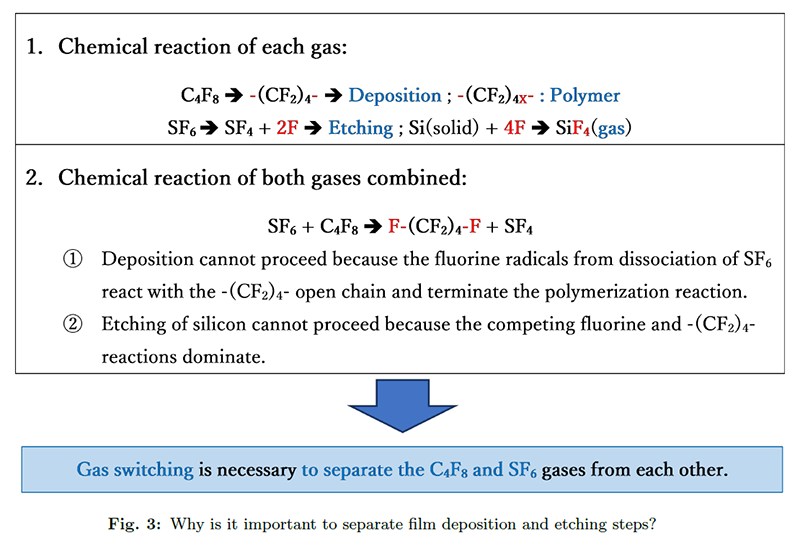
The ring structure of C4F8 is broken and the chain-shaped C4F8 is generated in plasma. The polymerization reaction occurs when -(CF2)4- groups react with each other to form longer chains. The polymer forms the passivating film on the surfaces of the etched trenches. In the presence of SF6, the fluorine radicals from the dissociation of SF6 react with the chain -(CF2)4- groups and terminate the polymerization reaction. In addition, the fluorine radicals disappear as they are consumed by the termination reaction and thus, etching cannot occur. In summary, a quick gas switching every 0.1 sec is used to avoid the mixing of C4F8 and SF6 gases.
4 Different sidewall profiles with Bosch process.
Is the Bosch process easily realized by repeating the three steps? It is actually difficult and there are some Bosch process specific problems. Because step 3 of the Bosch process (Silicon etching process) is a chemical reaction with fluorine radicals, the etch rate is highly dependent on the aperture area of exposed silicon. This is often referred to as the loading-effect. Also, as the aspect ratio increases, the probability of fluorine radicals being transported to the bottom of the trench or hole is reduced. This results in pattern-dependent etch effects, which is generally referred to as micro loading that adversely affects depth uniformity. Micro loading results from the depletion of reactants when the wafer has local, higher-density areas. In addition, DRIE-specific problems include notching when etching SOI (Silicon on Insulator) wafers and tilt due to non-uniform plasma distribution. These problems are addressed by adjusting system hardware, process parameters and device structure.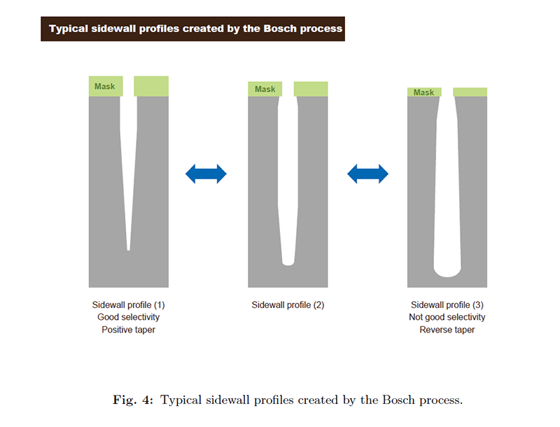
Fig. 4 shows the different sidewall profiles that can be engineered with the Bosch process.
- The sidewall profile directly under the mask is vertical. It becomes gradually taper to the bottom.
- The sidewall profile directly under the mask is a reversed taper. It becomes vertical, and gradually tapers as the aspect ratio or etch depth increases.
- Reversed taper sidewall profile.
As long as the Bosch process is run, the etch feature will end up with one of the sidewall profiles, or the sidewall profile obtained by cutting off the upper part of that etch feature. For example, if vertical sidewall profile is needed, the top part of etch feature (1) can be cut and used.
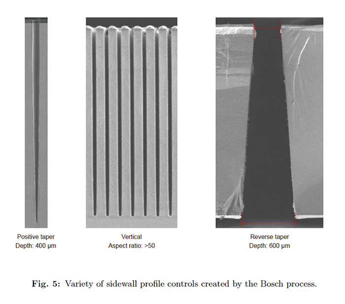
Since the Bosch process is made up of three different steps, there are three times as many parameters as conventional ICP etching processes. This allows the Bosch process far more flexibility, but also increases the time needed to tune all of its process parameters. Samco has extensive knowledge and process know how with the Bosch process that enables us to better support our customers in the DRIE application space. Fig. 5 are process examples of different sidewall profiles achievable in our DRIE systems.
References
- Kokkoris, G., Goodyear, A., Cooke, M. and Gogolides, E. A global model for C4F8 plasmas coupling gas phase and wall surface reaction kinetics, Journal of Physics D: Applied Physics, 41, 19 (2008), 195211.
- Laerme, F., Schilp, A., Funk, K. and Offenberg, M. Bosch deep silicon etching: improving uniformity and etch rate for advanced MEMS applications, Technical Digest. IEEE International MEMS 99 Conference. Twelfth IEEE International Conference on Mi- cro Electro Mechanical Systems (Cat. No. 99CH36291)IEEE (1999).
- Nagaseki, K., Kobayashi, H., Ishikawa, I., Nishimura, E., Saito, Y. and Sug- anomata, S. Mass spectrometry of discharge products at 13.56 MHz in SF6 gas, Japanese journal of applied physics, 33, 7S (1994), 4348.
- Rangelow, I. W. Critical tasks in high aspect ratio silicon dry etching for microelec- tromechanical systems, Journal of Vacuum Science & Technology A: Vacuum, Surfaces, and Films, 21, 4 (2003), 1550-1562.
- Wu, B., Kumar, A. and Pamarthy, S. High aspect ratio silicon etch: A review, Journal of applied physics, 108, 5 (2010), 9.

What the Samco Si-DRIE Can Do?
Anisotropic Silicon Deep Reactive Ion Etching process using the Bosch Process and Non-Bosch Process enables trench, hole and pillar fabrication for various device applications. These are some examples of structures fabricated using the Bosch Process. For more details, please visit the processes below.
Samco Product Portfolio for Silicon Deep Reactive Ion Etching
Our systems have industry-leading process capabilities, and the product lineup covers both R&D and production.