High-Precision Etching
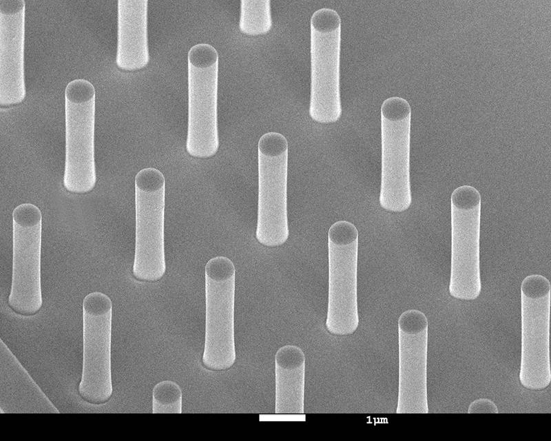
High-aspect-ratio Indium Phosphide (InP) micro- and nanopillars are foundational structures for next-generation optoelectronic and photonic integrated devices. In applications such as semiconductor lasers and photonic crystals, controlling light propagation and minimizing scattering losses require exceptionally vertical profiles with high sidewall and bottom-surface quality. Samco's Inductively Coupled Plasma (ICP) dry etching technology provides precise, high-anisotropy pattern transfer for InP pillar fabrication. The process achieves a distinct pillar structure with a diameter of 0.7 µm and a depth of 4 µm (aspect ratio > 5.5). The resulting profile features strictly vertical sidewalls with virtually no surface roughness or chemical residue, alongside a clean, smooth bottom surface free from trenching or degradation. This profile and surface integrity make the process an optimal solution for critical device features in optical communications, sensing, and quantum photonics, supporting seamless transition across both Lab and Fab environments.
Tweet