Atomic Layer Etching
Atomic Layer Etching (ALE) is a critical manufacturing process for advanced GaN/AlGaN power electronic devices and High Electron Mobility Transistors (HEMTs). As device dimensions shrink, conventional reactive ion etching (RIE) often causes surface damage, crystal defects, and non-uniform threshold voltages. ALE overcomes these processing limitations through a self-limiting cyclical reaction, enabling atomic-scale precision, low surface degradation, and high depth uniformity.
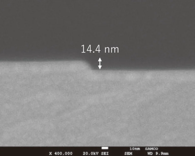
Samco's plasma ALE process utilizes alternating cycles of chlorine based modification and low-energy argon ion removal. Using a SiN hard mask (removed post-process), a 500 nm wide trench reached a depth of 14.4 nm after 88 cycles, delivering a precise etch rate of 1.63 Å/cycle. This atomic-scale depth control ensures uniform, damage-free pattern transfer for critical features such as gate recesses in GaN power HEMTs, RF amplifiers, and advanced AlGaN/GaN optoelectronic devices across both Lab and Fab applications.
Tweet