ICP Etching System RIE-400iPC
Precision 2", 3", 4" Compound Semiconductor ICP Etching
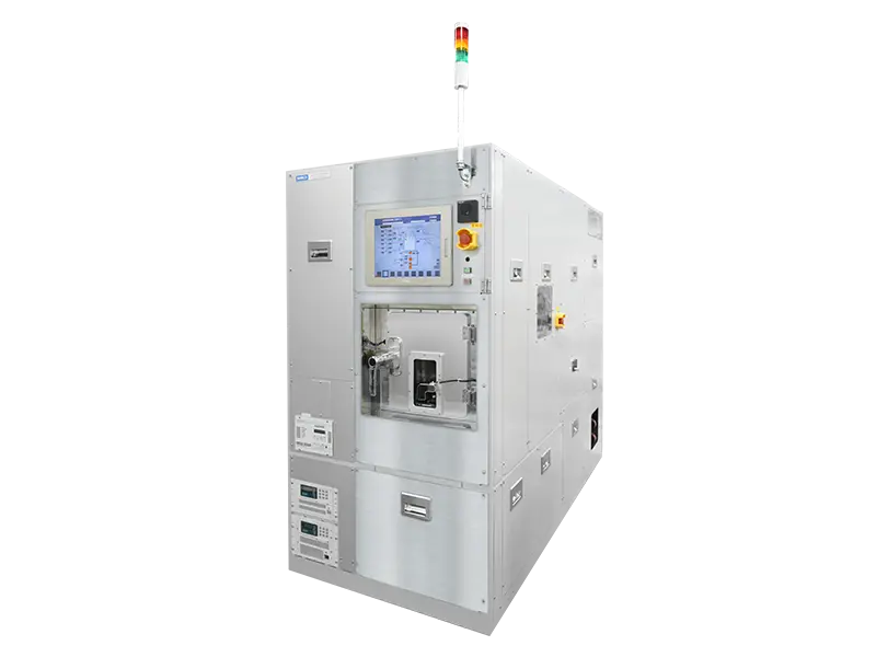
Description
The Samco RIE-400iPC is an automated cassette-loading Inductively Coupled Plasma (ICP) dry etching system optimized for compound semiconductor pilot lines, specialized foundries, and advanced research facilities. Engineered for substrates up to 4-inch (100 mm), the system combines automated vacuum cassette transport with high-density plasma generation to deliver anisotropic, low-damage etching across GaN, GaAs, SiC, and InP material systems.
Key Features and Benefits
- HSTC™ High-Power ICP Source: Integrates Samco’s proprietary HSTC™ (High-Density Surface Wave Inductively Coupled) ICP source for efficient, stable high-RF power coupling, generating high-density plasma under demanding high-power etching regimes.
- ESC & Helium Backside Temperature Control: Combines an Electrostatic Chuck (ESC) with backside Helium gas cooling to maintain precise, uniform substrate temperatures, preventing photoresist degradation and thermal mask erosion during aggressive etching.
- Direct-Coupled Vacuum Exhaust Architecture: Connects the vacuum exhaust system directly to the process chamber, securing a broad process window that spans from low-flow/low-pressure to high-flow/high-pressure regimes for wide process recipe flexibility.
- Direct Single-Wafer Transport (Ø2", Ø3", Ø4"): Supports automated carrier-tray-less single-wafer transfer for 2-inch, 3-inch, and 4-inch substrates, eliminating carrier-related particle generation and improving operational efficiency.
- Real-Time Endpoint Detection Options: Accommodates optional Optical Emission Spectroscopy (OES) or Laser Interferometry endpoint monitoring systems for precise real-time etch depth control and automatic process termination at heterojunction interfaces.
Applications
- InP Ridge Waveguide Patterning: Precision vertical sidewall etching for InP-based semiconductor lasers and photonic integrated circuits (PICs).
- InP Grating Formation: Fine-pitch, nanometer-scale profile control for Distributed Feedback (DFB) laser gratings.
- GaAs VCSEL Mesa Etching: Anisotropic mesa structure patterning with high mask selectivity and smooth sidewall morphology for GaAs-based VCSELs.
- High-Selectivity GaN/AlGaN Etching: Highly selective etch processing for AlGaN/GaN heterostructure layers with minimal sub-surface damage.
- GaN Gate Recess Etching: Low-damage, precise depth control for E-mode (normally-off) GaN HEMT gate recess fabrication.
- Vertical GaN Power Device Trench Etching: High-aspect-ratio trench formation with controlled sidewall profiles for vertical GaN power transistors.
- SiC MOSFET Trench Etching: High-rate, smooth trench patterning for next-generation SiC trench MOSFETs.
- Dielectric Etching (SiO2 / SiNx): Anisotropic, high-selectivity dry etching of dielectric hard masks and insulating thin films.
- Metal Etching: Residue-free dry etching of metallic electrode layers, contact pads, and hard mask metals.
Papers & Publications
- Kondo, Takaaki, Yoshihiko Akazawa, and Naotaka Iwata. "Effects of p-GaN gate structures and fabrication process on performances of normally-off AlGaN/GaN high electron mobility transistors." Japanese Journal of Applied Physics 59.SA (2019): SAAD02.
- Raj, Vidur, et al. "High-efficiency solar cells from extremely low minority carrier lifetime substrates using radial junction nanowire architecture." ACS nano 13.10 (2019): 12015-12023.
Related Products
Explore more products in ICP Etching Systems



