ICP Etching System RIE-800iPC
High-Uniformity ICP Etching System with Automated Cassette Loading
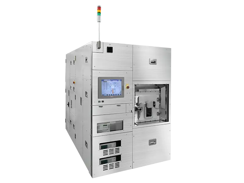
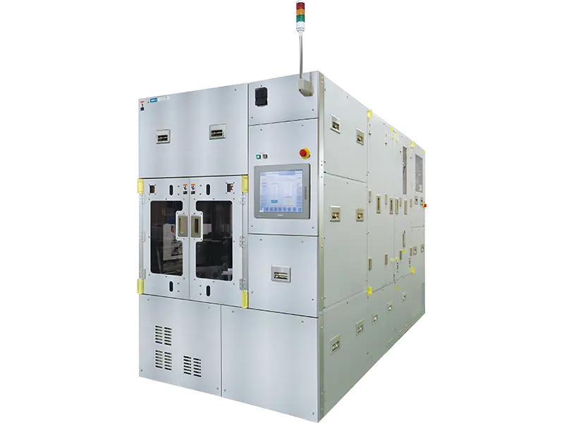
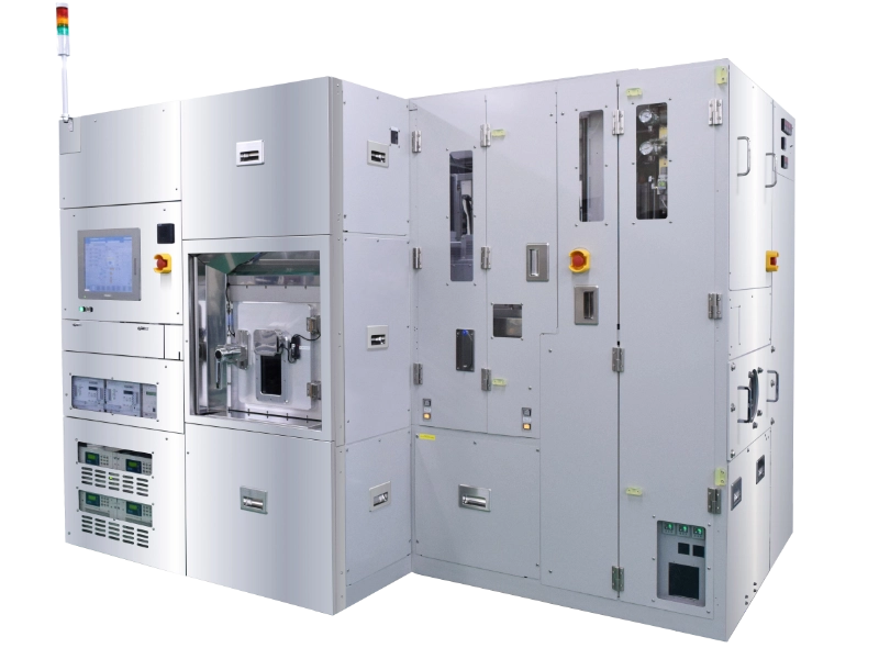
Description
The RIE-800iPC is Samco’s flagship inductively coupled plasma reactive ion etching (ICP-RIE) system, specifically engineered for high-volume manufacturing and advanced process development on up to 8-inch substrates. Integrated with a fully automated vacuum cassette chamber, the system isolates the process chamber from atmospheric exposure, minimizing moisture ingress and particle contamination to guarantee batch-to-batch process repeatability.
Key Features and Benefits
- HSTC™ High-Power ICP Source: Incorporates Samco's proprietary HSTC™ (Hyper Symmetrical Tornado Coil) ICP source to deliver efficient and stable high-RF power coupling (2 kW or more), generating high-density, highly uniform plasma over the entire Ø8-inch processing area.
- Adjustable Lower Electrode Elevation Mechanism: Features a motorized vertical stage mechanism to optimize the substrate-to-plasma gap distance, securing uniform electric field distribution and superior in-plane etch rate uniformity.
- Direct-Coupled High-Flow Vacuum Exhaust: Utilizes a high-conductance vacuum exhaust system connected directly to the process chamber, establishing a broad operational window that spans from low-flow/low-pressure regimes to high-flow/high-pressure regimes.
- ESC & Helium Backside Thermal Management: Combines an Electrostatic Chuck (ESC) with backside Helium gas cooling to maintain precise, stable substrate temperature control, preventing photoresist degradation and thermal mask erosion during aggressive physical etching.
- Advanced Real-Time Endpoint Detection Options: Supports optional Optical Emission Spectroscopy (OES) or Laser Interferometry endpoint monitoring for real-time etch depth control and automatic process termination at heterojunction interfaces.
Applications
- High-Selectivity GaN/AlGaN Etching: Highly selective etch processing across AlGaN/GaN heterostructures with minimal sub-surface lattice damage for RF and power electronics.
- GaN Gate Recess Fabrication: Low-damage, atomic-scale depth control for E-mode (normally-off) GaN HEMT gate recess processes.
- Vertical GaN Power Device Trenching: High-aspect-ratio trench formation with controlled sidewall taper angles for vertical GaN power transistors.
- SiC MOSFET Trench Etching: High-rate, smooth sidewall trench patterning for high-voltage SiC power MOSFETs.
- GaAs VCSEL & InP Photonics Processing: Smooth mesa sidewall fabrication and grating/waveguide formation for VCSELs, DFB lasers, and photonic integrated circuits (PICs).
- Dielectric Patterning (SiO2 / SiNx): High-rate, anisotropic dry etching of dielectric hard masks and inter-layer insulating films.
- Ferroelectric & Noble Metal Etching: Residue-free etching of difficult-to-etch materials, including ferroelectrics (PZT, BST, SBT) and metal electrode stacks (Pt, Au, Ru, Al, Cr, Ni).
Related Products
Explore more products in Etching Systems



