


Optoelectronics that use Gallium Arsenide (GaAs) wafers, such as light emitting diodes (LEDs), laser diodes (LDs) and Vertical Cavity Surface Emitting LASERs (VCSELs), are widely used for various indicators, optical disks and infrared communications. The result has been the miniaturization of products, which has led to the miniaturization of corresponding devices and improved wafer efficiency.
Cutting these wafers into chips generally involves diamond scribing and dicing blades. However, such techniques create a host of problems, including 1) loss of usable wafer area because of the dicing width, and 2) physical or heat damage to the devices, making yield rates suffer as a result.
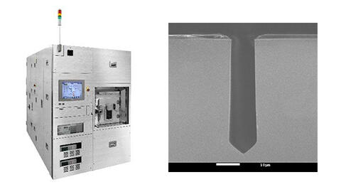
This article introduces a GaAs plasma scribing technique that uses an ICP etching system to solve these problems with narrow scribing widths, a complete lack of chipping, and scribe lines with an innovative V-shaped bottom that all result in easy breaking of GaAs.
To continue, please submit the form.