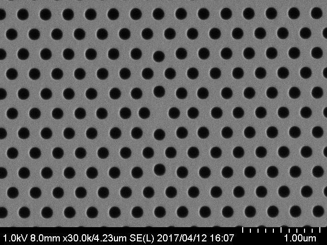
GaAs ICP Etching
Integrating semiconductor quantum dots (QDs) with optical nanocavities is essential for advancing quantum photonic devices and quantum information processing. Achieving strong light-matter interaction requires maximizing the Purcell factor by combining a high quality factor (Q) with an ultra-small modal volume (V). Fabricating these nanoscale architectures requires anisotropic dry etching capable of producing precise nano-hole arrays while preventing optical scattering losses and lattice damage. Samco's Inductively Coupled Plasma (ICP) etching systems provide chlorine- and fluorine-based dry etching solutions optimized to meet the strict nanoscale requirements of Photonic Crystal processing.
Photo Courtecy
Tweet