


Samco, a leading manufacturer of etching, deposition and surface treatment processing equipment for the semiconductor and related industries and academic facilities, is proud to introduce the new plasma etching cluster tool "Cluster H™." "With our cutting-edge plasma etching technology, Cluster H™ provides the full-scale production capabilities for compound semiconductor devices such as high-frequency filters, SiC/GaN power devices, GaAs VCSELs, micro-OLED/LED, CMOS image sensors, and advanced packaging," explains Tsukasa Kawabe, President and COO of Samco. "We created Cluster H™ to meet the strong demand from our valued customers for high throughput equipment. Cluster H™ with etching processes available only at Samco enables the combination of optimal materials and process technologies in advanced electronic device fabrication" continues Tsukasa.
■System photo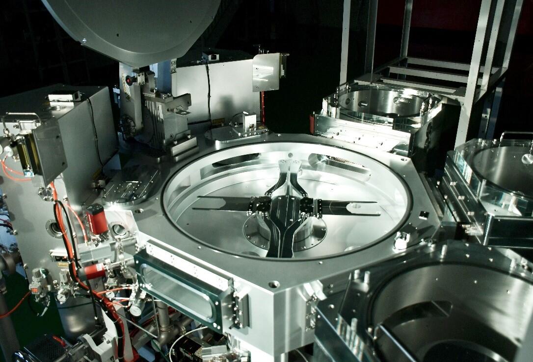
Cluster tool system "Cluster H™" for fabrication of compound semiconductor devices such as high-frequency filters, SiC/GaN power devices, GaAs VCSELs, micro-OLED/LED, CMOS image sensors, and advanced packaging.
■Specifications
|
Model |
H6 / H8 |
|
Sample Size |
ø6" (ø150 mm) / ø8" (ø200 mm) |
|
Processes |
Etching and Ashing |
|
Number of Chambers |
Up to three reaction chambers / process modules |
|
Number of Cassette Stages |
Two (cassette modules) |
|
Number of Wafer Aligners |
One (positioned between cassette module and transfer chamber) |
■Features
Cluster H™ is a cluster tool for etching and ashing that supports direct transfer of ø6" and ø8" diameter wafers. Centered on a hexagonal vacuum transfer platform, it is equipped with two vacuum cassette chambers and one vacuum aligner as part of the standard equipment configuration, and up to three process modules that can be attached. The ICP etching process module uses the reaction chamber of the high-end ICP etching model RIE-800iP and is backed by our extensive process library and best-known methods. In addition, the frog-leg dual-blade robot enables high wafer throughput, compact transfer chamber, and system footprint.
In addition, the revamped software incorporates useful functions with improved reliability. The standard system is equipped with a user-friendly GUI and equipment management functions such as equipment performance tracking, wafer transfer history for each module and packages, and simulation functions for higher-level communication, and supports the manufacturing execution system (MES) used at customers' factories.
■Equipment configuration example (three-etching process modules)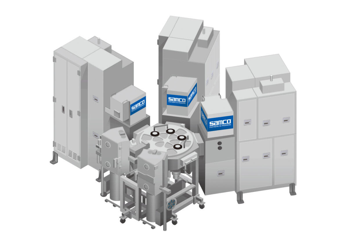
Samco announces the release of the production-worthy cluster tool, Cluster H™. The system is ideally suited for high volume manufacturing leveraging our experience and expertise in manufacturing production-proven systems and our broad process know-how. With the advanced hardware and software features on the Cluster H™, we are certain that it will contribute to the success in manufacturing of electronic devices for our valued customers. As a pioneer in thin film technology, Samco looks forward to continuing to provide cutting-edge solutions to the industry.
About Samco Inc.
Samco Inc. (TSE: 6387) stands for Semiconductor And Materials Company, and is a leading manufacturer of processing equipment for the semiconductor and related industries founded by Mr. Osamu Tsuji in Kyoto, Japan in 1979. Over the past forty-three years, more than 4,300 Samco systems have been installed and used in 35 different countries. Its equipment and thin film technology are widely adopted in the fabrication of semiconductor devices, including high-frequency filters, SiC/GaN power devices, GaAs VCSELs, micro-OLED/LED, CMOS image sensors, MEMS, TSVs, advanced packaging, and so on. Learn more at www.samco.co.jp/en/.
Company Contacts:
TSUCHIHASHI, Atsushi
Public Relations
Phone: 81-75-621-7841
E-mail: tsuchihashi@samco.co.jp